TSMC's 2nm Breakthrough Powers the Next Wave of AI and Mobile Tech
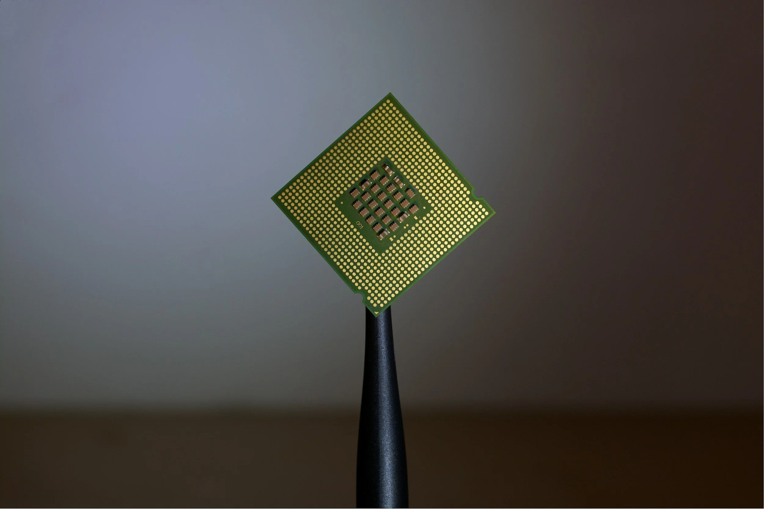
Image Credit: Brian Kostiuk | Unsplash
On the eve of its second-quarter earnings conference, Taiwan Semiconductor Manufacturing Company (TSMC) received a significant boost in performance expectations. NVIDIA has increased its AI GPU foundry orders with TSMC by 25%, signaling robust demand for AI technologies. Additionally, Apple is set to be the first customer for TSMC's pioneering 2nm process technology, earmarked for the upcoming iPhone 17. These developments underscore TSMC’s pivotal role in shaping next-generation technology landscapes.
Advancing AI GPU Production with the Blackwell Architecture
NVIDIA is enhancing its AI GPU production through a partnership with TSMC, utilizing the advanced Blackwell architecture to meet a surging global demand. This collaboration has led to a 25% increase in NVIDIA's order volume, underscoring the significant market appetite for high-performance AI computing. The Blackwell architecture, which integrates 208 billion transistors and utilizes TSMC's custom 4NP process, is a monumental advancement in AI technology. Each GPU within this architecture includes two reticle-limited dies connected via a 10TB/s chip-to-chip interconnect, facilitating exceptional performance across applications like large language models and Mixture-of-Experts models. The sophisticated second-generation Transformer Engine and innovative Tensor Cores further enhance this capability. NVIDIA's commitment to security is evident through its Confidential Computing features, which safeguard data and AI models without compromising throughput. The architecture's efficiency is amplified by the fifth-generation NVIDIA NVLink, which supports up to 576 GPUs for improved communication and processing power, essential for handling trillion-parameter AI models. Additionally, the Blackwell platform is equipped with a high-speed Decompression Engine and a dedicated RAS Engine for predictive management, ensuring reliability and minimizing downtime in crucial AI operations. TSMC's cutting-edge manufacturing capabilities are crucial in realizing the potential of the Blackwell architecture, pushing the boundaries of AI hardware performance.
Apple's First Mover Advantage with TSMC’s 2nm Process
Apple will pioneer the adoption of TSMC's 2nm process technology, showcasing their continued partnership in innovating mobile technology. This collaboration not only highlights Apple's commitment to maintaining a technological edge in its products but also underscores TSMC's role as a leader in semiconductor innovation. The 2nm chips are expected to enhance the performance and efficiency of Apple’s devices, setting new industry standards.
Advancements of High-NA EUV Lithography Machines
TSMC's deployment of the high-NA EUV lithography machine, developed by ASML, signifies a pivotal evolution in semiconductor manufacturing. This advanced technology enables the fabrication of chips with unprecedentedly small feature sizes, essential for developing the cutting-edge 2nm process and further advancements. High-NA EUV lithography uses extreme ultraviolet (EUV) light with a wavelength of 13.5 nm and increases the numerical aperture (NA) from 0.33 to 0.55, allowing the new EXE systems to achieve critical dimensions (CD) as small as 8 nm. This nearly doubles the transistor density achievable with previous NXE systems and is crucial for enhancing the performance and capabilities of next-generation chips from leaders like NVIDIA and Apple. The technology's innovative anamorphic optics, which magnify the pattern differently in two directions, address challenges related to light reflectivity at steeper angles, thus maintaining the usability of standard-sized reticles. This breakthrough is expected to significantly boost the potential of future digital technologies, including robotics, AI, and IoT devices, by supporting the production of extremely dense logic and memory chips, reinforcing TSMC's supremacy in the global semiconductor market.
Strategic Developments in AI and Mobile Chipsets
TSMC is not just increasing its production capabilities but also expanding its technological horizons with developments in advanced 3D packaging. The SoIC technology planned for Apple's M5 chip highlights TSMC’s innovative approaches to meeting the complex demands of modern chip architectures. This strategic focus on advanced packaging and process miniaturization is set to transform the efficiency and functionality of AI and mobile devices. SoIC (System on Integrated Chips) enables the stacking of multiple chips vertically, reducing the footprint and enhancing performance through shorter interconnects. This technology incorporates hybrid bonding, including copper-to-copper connections and through-silicon vias, allowing for denser interconnect packing and higher bandwidth. SoIC’s flexibility supports the integration of various chip types in a single package, crucial for AI processing and mobile device compactness. This advancement is critical for devices requiring high performance and energy efficiency, driving forward the capabilities of AI applications and mobile computing.

